
For readers new to the name, ASML is the company that makes the machines that let the world’s most advanced chips exist. Without it, “cutting-edge” semiconductors would stall.
TL;DR
What it does: ASML builds photolithography systems—industrial scanners that pattern nanometer-scale features on silicon. It is the only supplier of EUV (extreme-ultraviolet) tools required for the most advanced nodes.
Why it matters: AI, data centers, and advanced memory are driving a new wave of lithography intensity (more layers, tighter tolerances). ASML sits at that choke point.
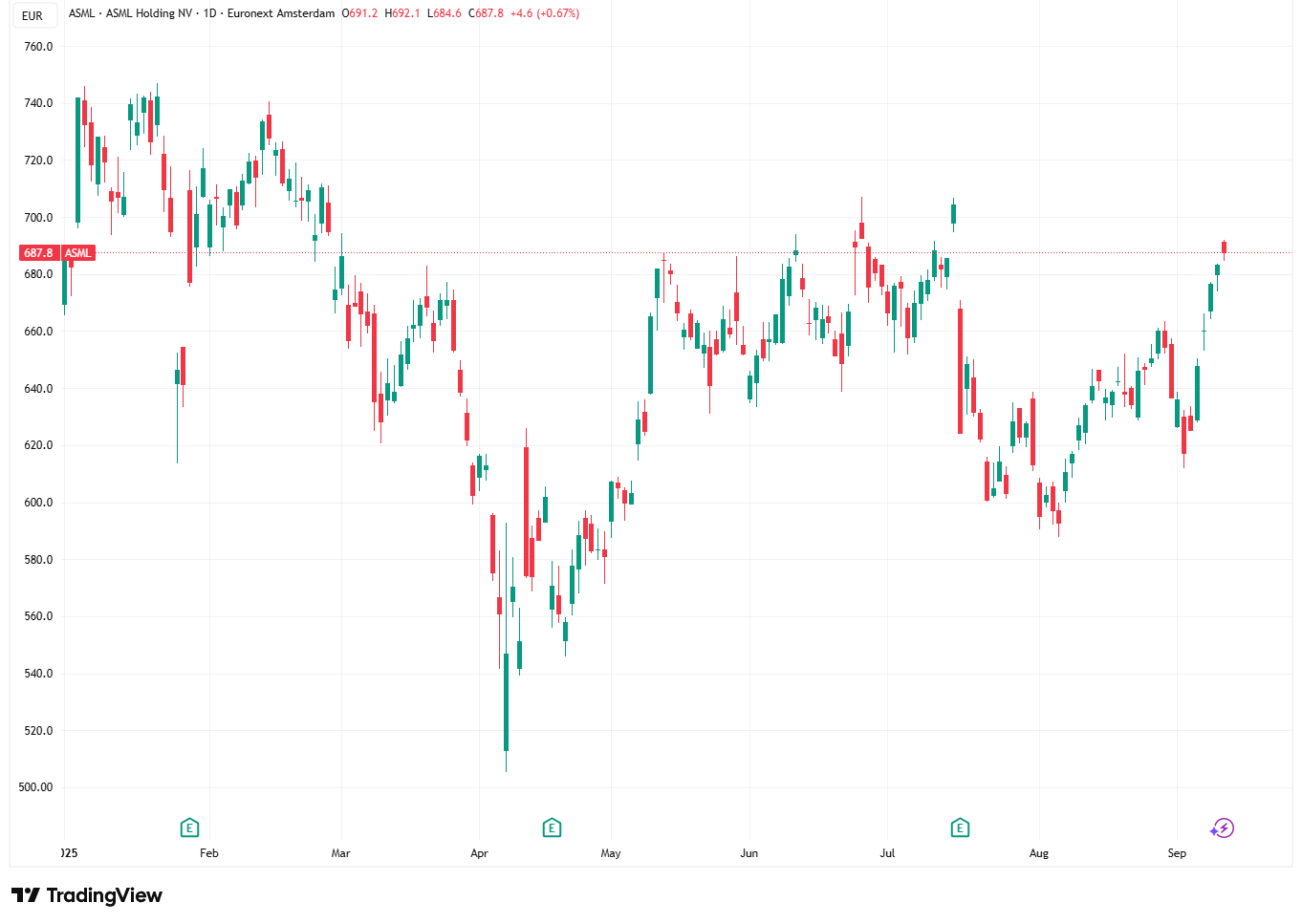
2025 snapshot: Q2 revenue €7.7bn, gross margin 53.7%, net bookings €5.5bn; order backlog ~€33bn; full-year 2025 sales expected +~15% with GM ~52%. EUV revenue seen ~+30% YoY in 2025.
Next leg: Transition to High-NA EUV (0.55 NA) is underway; the first EXE:5200B has been shipped and being installed, enabling single-exposure patterning beyond Low-NA EUV.
Wild cards: Export controls (esp. China), tariff policy, customer capex timing—and the cadence of AI/Memory nodes.
What ASML Actually Makes (and why it’s unique)
ASML builds the ultra-precise “printers” (lithography scanners) that project circuit patterns onto silicon wafers at nanometer scales. Every modern chip—CPU, GPU, DRAM, NAND—passes through these machines dozens of times. As features shrink, you need shorter wavelengths of light and more exact optics to keep drawing lines cleanly and in the right place.
Lithography 101 (the essentials that drive economics):
Resolution depends on wavelength and numerical aperture (NA). Shorter wavelength and higher NA → finer features.
Overlay is how accurately each new layer lines up with the previous ones—this is crucial for yield.
Throughput & uptime determine cost per wafer; fabs need high wafers-per-hour with stable availability.
ASML’s product stack
DUV (Deep-UV) immersion—workhorse scanners.
ArF immersion systems (e.g., NXT:2000i/2050i/2100i) use 193 nm light and a thin layer of water between the lens and wafer to boost NA. They handle a large share of layers in logic and memory, including many non-critical steps, and remain economically vital even at advanced nodes.EUV (Extreme-UV) for cutting-edge layers.
The NXE family uses 13.5 nm light and reflective optics (mirrors instead of lenses) inside a vacuum chamber. EUV lets chipmakers print the most demanding layers with fewer patterning steps. The latest NXE systems achieve very high productivity (hundreds of wafers per hour in the field), which is what makes EUV commercially viable rather than just a lab curiosity.High-NA EUV (next resolution jump).
The EXE platform raises NA from ~0.33 (Low-NA EUV) to 0.55, increasing resolution and reducing multi-patterning on the hardest layers. That means fewer passes, lower defect opportunities, and better cycle time—i.e., improved cost per transistor. High-NA introduces new optics (anamorphic imaging) and mask requirements and is the path beyond the 2 nm era.Holistic lithography (the control loop).
Scanners are only part of the story. ASML wraps them with:
• Metrology (e.g., YieldStar) to measure focus/overlay and feed corrections,
• E-beam inspection (via HMI) to find defects at tiny scales, and
• Computational lithography/software to predict and correct imaging distortions.
This “measure–analyze–correct” loop is how fabs push performance, yield and throughput simultaneously.
Why only ASML at the frontier?
EUV light generation is extreme. A high-power industrial laser strikes droplets of tin to create a hot plasma that emits EUV at 13.5 nm. Capturing that faint light efficiently and consistently—shot after shot—is a major systems challenge.
No lenses at EUV—only mirrors. Conventional glass absorbs EUV, so ZEISS SMT builds multi-layer mirror stacks with atomic-level precision. Each reflection must preserve wavefront quality; there’s no margin for contamination or misalignment.
Vacuum, cleanliness, and materials science. EUV requires ultra-high vacuum, specialized pellicles (protective membranes) for masks, and resists tuned to minimize stochastic defects. Every component interacts; improving one often forces changes elsewhere.
System-of-systems integration. The EUV ecosystem includes TRUMPF lasers, ZEISS optics, Cymer light sources (owned by ASML), resist suppliers, mask shops, and fab tooling. ASML is the orchestrator—co-developing specs, synchronizing upgrades, and qualifying end-to-end performance in customer fabs.
Learning curves and installed base. Decades of iteration with top customers (and thousands of field upgrades) compound into know-how that’s hard to replicate. Each new tool benefits from this accumulated data and process tuning.
Bottom line: ASML doesn’t just sell machines; it delivers a tightly integrated lithography platform—scanner, metrology/inspection, and computational correction—engineered to push physical limits while hitting fab economics. That integration, plus the sheer difficulty of EUV, is what makes the company uniquely positioned at the heart of advanced semiconductor manufacturing.
Where We Are in 2025
High-NA EUV (EXE, 0.55 NA). Next-gen EUV platform that increases resolution and reduces multi-patterning on the toughest layers. Designed to lower cost-per-transistor and extend scaling beyond ~2 nm as uptime and throughput mature.
EUV (NXE, 13.5 nm). ASML’s flagship scanners for leading-edge layers in logic and advanced memory. EUV replaces complex multi-patterning with fewer exposures, improving cycle time and defectivity at the smallest geometries.
DUV ArF Immersion (193 nm). High-throughput workhorses that use a thin water layer to raise numerical aperture and resolution. They print a large share of non-critical and semi-critical layers across logic and DRAM, even at advanced nodes.
ArF Dry (193 nm). DUV scanners without immersion, optimized for less demanding layers where cost and simplicity matter. Common in mature nodes and supportive layers in advanced flows.
KrF (248 nm). Reliable DUV tools for larger-geometry and mature-node manufacturing. Widely used for implant, contact, and back-end layers where extreme resolution isn’t required.
i-line (365 nm). Legacy wavelength systems focused on coarse features and specialty processes (e.g., analog, power, sensors). Favoured for cost-efficient production at older nodes.
Metrology & Inspection (Holistic Lithography). Software-driven measurement and e-beam inspection that monitor overlay, focus, and defects, feeding real-time corrections to scanners. This control loop lifts yield, availability, and cost efficiency across the installed base.

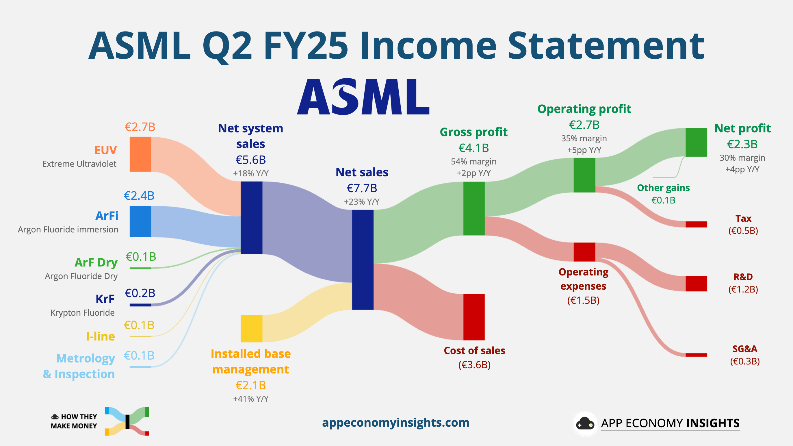
Financials & demand signals (Q2 2025):
Net sales: €7.7bn; GM: 53.7%; net bookings: €5.5bn (≈€2.3bn EUV).
Backlog: ~€33bn (after a €1.4bn adjustment tied to 2024 export-control responses).
FY25 guide: total sales +~15% vs 2024; GM ~52%; EUV revenue ~+30% YoY driven by higher NXE:3800E productivity and initial High-NA revenues.
Technology cadence:
First EXE:5200B High-NA system shipped and being installed; the goal is single-exposure patterning where Low-NA required multi-patterning. Management frames High-NA as a cost-of-technology improvement, not just resolution.
Customers & mix:
Leading customers include TSMC, Samsung, Intel, SK hynix, among others. China’s share of 2025 sales has been stronger than anticipated, trending “a little over 25%” earlier this year, though expected to normalize to backlog over time.
Revenue Segmentation: End-use and Geography (H1 2025)
By end-use (sector proxy). In the first half of 2025, ASML’s total net sales were €15.43bn, split between Logic ~46% (€7.16bn), Memory ~27% (€4.18bn), and Installed Base Management (services & upgrades) ~27% (€4.10bn). This mirrors the industry’s lithography intensity: logic drives critical-layer EUV demand while DRAM adds layers via HBM roadmaps; services scale with every tool in the field.
By geography. Sales remain heavily Asia-centric given where leading-edge fabs are located. South Korea ~28.6% (€4.41bn), Taiwan ~28.3% (€4.36bn), China ~24.1% (€3.71bn), United States ~12.6% (€1.94bn), Japan ~3.2% (€0.49bn), EMEA ~2.0% (€0.31bn), Singapore ~1.3% (€0.19bn) for H1 2025. Note: ASML attributes revenue to the location of the customer’s fab, so mix can be lumpy quarter-to-quarter with shipment timing.
By product/technology (context for the mix). Within net system sales (€11.34bn), EUV (NXE) ~49%, DUV ArF immersion ~38%, High-NA EUV (EXE) ~2%, with the remainder from ArF dry, KrF, i-line and Metrology & Inspection. This underscores EUV’s centrality while High-NA begins to contribute.
Strategic Moat
Sole-source EUV with deep co-development across the stack (optics, sources, resist ecosystem).
Throughput economics: NXE:3800E field upgrades to ~220 wph and rising High-NA productivity (EXE:5200B ~+60% vs EXE:5000) improve cost/wafer.
Installed base annuity: Services/upgrades (Installed Base Management) exceeded €2.0bn in Q2 alone—growing with every tool shipped.
Learning curve & supplier web: tightly coupled partners (ZEISS, TRUMPF, Cymer) and decades of EUV learning make replication extraordinarily difficult.
Catalysts That Matter
AI & memory: More EUV layers in DRAM (HBM roadmaps) and advanced logic nodes increase lithography intensity through the decade.
High-NA adoption: Initial customer deployments set up a 2027–2029 ramp as processes mature; industry interest spans logic and DRAM.
Geopolitics & policy: Dutch export-control updates (effective April 1, 2025) and U.S. rule changes continue to shape shipment eligibility; ASML has said the recent updates fit within its 2025 outlook.
Constraints & Risks
Export controls/tariffs: Policy can delay orders/shipments; management could not confirm 2026 growth given macro/geopolitical uncertainty.
Customer capex timing: Foundry/IDM spend can bunch or pause with node transitions, regional incentives, or tariff outcomes.
Execution: High-NA industrialization (uptime, overlay, pellicles) must meet fab economics at scale.
Supply chain depth: Optics and laser subsystems are highly specialized; partner bottlenecks could cap unit output.
The Investment Debate (Framed, not a recommendation)
Bull case (what supporters argue):
Chokepoint economics. ASML’s effective monopoly in EUV gives it structural pricing power and outsized strategic relevance as lithography intensity rises (more EUV layers per wafer across advanced logic and HBM-driven memory). Even if wafer starts wobble cyclically, node migration keeps pushing critical layers onto EUV, sustaining tool demand, upgrades and service revenue. The company’s role as coordinator of a uniquely complex supplier web (optics, sources, pellicles, computational lithography) further entrenches its position and raises switching costs.
High-NA unlock. Moving to 0.55 NA enables single-exposure patterning on layers that otherwise require multi-patterning, cutting steps, cycle time, defect opportunities and fab energy footprint. If High-NA achieves stable uptime and target throughput, cost-per-transistor should improve, widening the economic moat while extending the scaling roadmap beyond 2 nm. Early customer insertions also create a multi-year learning-curve advantage that competitors cannot easily compress.
Compounding annuity. Every tool shipped expands a high-margin installed base that throws off recurring services, field upgrades (throughput/overlay), software, metrology and e-beam inspection revenue. This annuity tempers WFE volatility, increases visibility, and deepens customer lock-in as fabs standardise around ASML’s holistic lithography stack. Over time, mix shift toward services can support resilient gross margins and cash conversion.
Bear case (what skeptics argue):
Policy shock risk. Export-control scope changes or new tariff regimes can delay shipments, force reconfigurations, or restrict service access, particularly where China mix is meaningful. Even if headline guidance absorbs known rules, licensing uncertainty can weigh on bookings timing and supply-chain planning, creating lumpiness and operational friction. A more fragmented global semiconductor policy landscape could also raise compliance costs structurally.
Capex cyclicality. If AI server digestion extends or memory pricing underwhelms, customers may push out tool deliveries and slow backlog conversion. Foundry/IDM budgets remain sensitive to end-demand signals, yields at new nodes, and regional incentive milestones—any of which can compress near-term orders and utilisation. In a softer macro, even a strong long-term thesis won’t fully shield near-term WFE downshifts.
Execution at the frontier. High-NA must clear real-world hurdles—pellicle durability, photoresist chemistry, stochastic defectivity, source power, overlay and uptime—to hit the fab-level cost targets that drive broad adoption. Bottlenecks at critical suppliers (mirrors, lasers, precision modules) could cap output just as demand intensifies. If throughput or availability trails expectations, customers may defer insertions and rely longer on refined Low-NA multi-patterning.
What to Watch (practical checklist)
Bookings vs. ship sets by end-market (logic vs. memory) and region.
High-NA milestones: additional EXE:5200B recognitions, customer site installs, and declared insertion nodes/timelines.
Installed base growth: service revenue run rate and upgrade mix (NXE:3800E productivity upgrades).
Policy updates: Dutch licensing scope changes, U.S. rule amendments, and any tariff outcomes affecting 2026 capex.
Bottom Line
ASML is not “just another semiconductor stock”—it is the enabler of advanced manufacturing. 2025 is tracking as a healthy growth year (~+15% sales, ~+30% EUV), with the High-NA era beginning to move from labs into fabs. The near-term caveat is policy and capex timing into 2026; the longer-term thesis remains anchored in AI-driven lithography intensity and an installed base that compounds.
Disclaimer: This article is provided for informational and analytical purposes only and does not constitute investment advice or a recommendation to buy or sell any financial instrument. The views expressed are those of the author, based on sources deemed reliable at the time of writing, and are subject to change without notice. We make no guarantees about the information's accuracy, completeness, or timeliness, and we are not liable for any losses from its use. Before making any investment decision, you should consult a qualified professional to assess your individual objectives, risk tolerance, and financial circumstances.